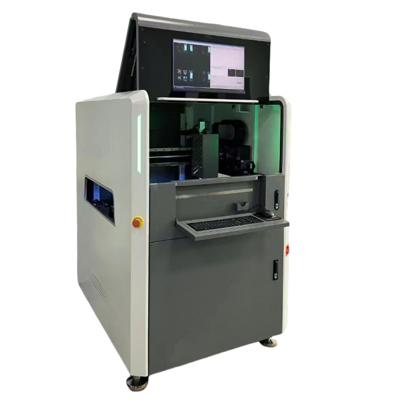
Online AOI PCB Automatic Optical Inspection Machine
High Precision-Multiple software analysis methods, multiple application modes, high-precision motion system;
High Efficiency-One matintenance workstation confirms the detection data of multiple online machines to realize full automatic process management and control.
Additional information
| Min. PCB Size | 50mm * 50mm |
|---|---|
| PCB Thickness | 0.6mm~6mm |
| Transmission Method | One Stage Lane |
| Camera | Gige Vision, Resolution 2448×2048 Mega pixels |
| Power | AC220V, 50/60HZ, 1.8KW |
Product Details:
- HD Color global exposure digital camera speed increase 30%
- High depth of field telecentric lens, which can measure the solder joints on the side of high components
- Support the detection of smt front, back and dip station
- Support 0201 packaged component inspection
- CAD data import, automatic linking component library, automatic color picking
- True non-stop offline programming and program update
- MES data docking to realize intelligent factory
- Support multi-line centralized management and remote service
Functional Features:
1, Global exposure Camera + telecentric lens
The global exposure camera has a faster exposure time than the roller shutter camera, which not only eliminates the dradding phenomenon of the roller shutter camera, but also increase the speed by more than 30%.
The telecentric lens solves the problem of wide-range lens image distortion and can easily deal with the detection of the side pads of high components, and in linear test, deflection angle test, distance test, it has more accurate effect.
2, Board bending compensation
When the board passes throught the oven, due to the difference in heat absorption by various types of components on the board, the board is unevenly heated, resulting in a certain degree of deformation of the board. The CAD coordinates and the position of the board after passing through the oven cannot be accurately matched. After the plate bending is compensated, the coordinates and the corresponding positions of the components accurate.
3, Reference point + Pad positioning + Body positioning
The industry’s strongest positioning menthod, easy to deal with a variety of severely deformed boards, especially for flexible boards, server motherboards and other products.
4, Comprehensive pad defect detection
Divide the pad into multiple arears, each arear has the characteristics of good and bad products, set the corresponding detection standards to measure.
5, Compatible with various shapes of pads
Wave soldering algorithm supports various shapes of pads, positioning is more accurate.
6, Offline programming systems & Operating system
True offline programming, non-stop debugging and updating procesures. Centralized management, one person and multiple machines, through remote network, can also realize remote service and machine adjustment.
|
影像系统 Image Parameters |
相机 Camera | 5MP/12MP Industry Camera | ||||||||
| 分辨率 Resolution | 5MP Camera: 15μm,10μm; 12MP Camera: 15μm,12μm,10μm,6.3μm | |||||||||
| FOV | 37*30mm(5MP,15μm); 60*45mm(12MP,15μm) | |||||||||
| 光源 Lighting System | Multi-angle Surrounding LED Light Source | |||||||||
| 运动机构
Movement System |
X/Y运动 | AC Servo | ||||||||
| 轨道调宽方式 | Auto | |||||||||
| 进板流向 | L-R / R-L(option) | |||||||||
| 硬件配置
Hardware |
操作系统 Operation system | Win 10 | ||||||||
| 通信方式 Communication Method | Ethernet, SMEMA | |||||||||
| 电源 Power Supply | 220V 50/60HZ 5A 0.4~0.6Mpa | |||||||||
| 轨道高度 Transmission Height | 900(+-20) | |||||||||
| 机器尺寸 重量 Weight Size | 1170*1608*1580 950KG | |||||||||
| 检查PCB规格 | 尺寸Size | 55*55mm | ||||||||
| 厚度 Thickness | 400*330 | 600*500 | 1200*500 | 400*300*2 | 600*300*2 | |||||
| PCB 重量 PCB Weight | 20mm/ 25mm | |||||||||
| 净高 Height | 630*1620*1470 | 830*1620*1470 | 1700*1150*1500 | 630*1620*1470 | 830*1620*1470 | |||||
| 板边 Board Edge | Windows 7 64 digit i7 CPU 16G 1TB 22‘ LCD (1920×1080) | |||||||||
| 检查项目 Inspection Content | 元件类defact content | Missing Parts, Misalignment,Tilted feet, virtual soldering, offset, pole reversal, tombstone, | ||||||||
| 焊锡类 solder paste | Bridging,less tin,More tin, floating pins bent pins, etc | |||||||||
| 检查元件 Checking Component | Chip:03015; LSI:0.3mm | |||||||||
| 检查速度Inspecting Speed | 180-200ms/FOV | |||||||||

